
Sticky Mat for Semiconductor Cleanroom | Advanced Control Solutions

Sticky Mat for Semiconductor Cleanroom | Advanced Control Solutions
Why Semiconductor Facilities Cannot Ignore Contamination Control
Even a particle that is a microscopic size can cause serious production problems in semiconductor manufacturing. One of the biggest threats to the yield, performance, and reliability of modern sticky mats for semiconductor cleanrooms with features in the nanometers is contamination.
- One particle that is transported on a shoe sole, equipment wheel, or trolley can penetrate a controlled environment and disrupt delicate production processes. This is why the contamination control starts much earlier than the personnel enter the manufacturing critical areas.
- One of the most effective and cost-effective contamination control devices is a sticky semiconductor cleanroom environment sticky mat. These mats are positioned at strategic entry points, and they trap dust, fibers, and particles before they get to sensitive production areas.
Understanding the Role of Sticky Mats in Semiconductor Manufacturing
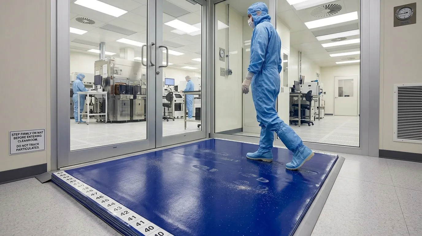
A sticky mat is a dust-catching adhesive mat that is installed at cleanroom entrances, gowning rooms, air showers, and transition zones. Each action on the adhesive surface eliminates contaminants that may otherwise move further into the facility. These mats are particularly helpful in:
• Cleanroom production of wafers.
• Semiconductor packaging operations
• Microelectronics production areas
• PCB assembly lines
• Research laboratory
Principle of Sticky Mat in Semiconductor Cleanroom
Multi-layer sticky semiconductor cleanroom mats have several sheets of adhesive that are stacked. The adhesive surface picks up: When operators cross the mat, the adhesive surface picks up:
• Dust particles
• Fibers
• Hair
• Packaging debris
• Dirt
• Fine particulate contamination
When the upper layer is saturated, it is peeled off to expose a new adhesive surface. This peel-off adhesive mat design ensures that its operation is regular and does not require cleaning or maintenance.
Industry testing and research indicate that correctly placed contamination control sticky mats can greatly decrease the movement of particles in footwear and rolling equipment. Nabai claims that up to 95 percent of the particulate matter on shoes and wheels can be removed by quality sticky mats before reaching controlled areas.
The Reasons Why Wafer Fabrication Facilities Require Special Sticky Mats
Semiconductor manufacturing is not similar to general manufacturing. The existing wafer production process comprises hundreds of steps that are accurate, including:
• Photolithography
• Etching
• Ion implantation
• Thin film deposition
• Chemical mechanical polishing
• Packaging and testing
Pollution at these levels can lead to:
• Pattern defects
• Yield loss
• Device failure
• Surface scratches
• Process variation
Wafer fabrication facilities have a cleanroom sticky mat that helps to reduce contamination transfer prior to the operator entering sensitive production areas. This is why numerous plants have numerous contamination control points during production.
Characteristics of the Ideal Sticky Mat in Semiconductor Cleanroom
- All Sticky Mats are Not Identical
A good sticky mat to use in a semiconductor cleanroom setting must have a number of desirable features.
- Good Particle Capture Efficiency
The high tack semiconductor cleanroom mat must be able to trap both the visible and microscopic particles without letting the contaminants enter the environment again.
- Low Residue Performance
A cleanroom low-residue sticky mat of semiconductor is applied to prevent any adhesive transfer to footwear, wheels, and cleanroom surfaces.
The pollution of residues can lead to its own working problems, and clean-removal adhesive technology is required.
- Multi-Layer Construction
A semiconductor cleanroom multi-layer sticky mat has a high service life. The operators do not have to change the entire mat frequently, but only peel off the dirty top. This will save on operational expenses without affecting the performance of the contamination control.
- Durable Polyethylene Construction
Polyethylene film is used in most high-quality mats because it provides:
• Excellent durability
• Consistent adhesive performance
• Low particle shedding
• Reliable cleanroom compatibility
Sticky mat technology of polyethylene is also one of the surest solutions in controlled environments.
Significance of ESD Protection in Semiconductor Facilities
The other major risk is the existence of static electricity. A discharge may be invisible and cause permanent damage to sensitive semiconductor devices. An electrostatic discharge protective contamination control mat is a semiconductor cleanroom ESD safe sticky mat.
These special mats can help support:
• Static dissipation
• Equipment protection
• Device reliability
• Process stability
ESD-safe solutions will provide additional protection against costly failures in the case of semiconductor manufacturing facilities. Nabai also manufactures ESD-oriented contamination control products, which are applied in the environment where particle control and management of the static environment are of paramount importance.
Placement Determines Effectiveness
A cleanroom entrance mat for semiconductor manufacturing should be installed.
• Main cleanroom entrances
• Air shower exits
• Gowning room transitions
• Material transfer zones
• Equipment access points
• Production area entryways
An effective location establishes an effective cleanroom ingress control plan. Several mats can be used in big facilities to create layered contamination prevention systems.
Advantages of Sticky Mats
A semiconductor cleanroom sticky mat is a disposable sticky mat that has a number of benefits.
- Consistent Performance
The new coating provides new adhesive power.
- Fast Maintenance
No cleaning or washing needed.
- Lower Downtime
The replacement of layers takes seconds.
- Better Compliance
Facilitates regular contamination control measures.
This makes disposable cleanroom mats a popular choice for semiconductor fabrication plants in the world.
Conclusion
Nabai offers a sticky mat for semiconductor cleanrooms, microelectronics manufacturing, and controlled environments in high tech. You might need an industrial cleanroom sticky mat, a semiconductor fabrication facility sticky mat, or a solution that fits your equipment. The Nabai team can help you build a cleaner, safer, and more productive facility. Visit the site of NABAI and request that they give you a customized solution to your operation.
NEWS
GET SERVICE
With quality parts to meet every budget and friendly staff trained to make your visit informative and hassle free.