
Sticky Roller for Semiconductor Adhesion Selection Guide

Sticky Roller for Semiconductor Adhesion Selection Guide
Choosing a Sticky Roller for Semiconductor manufacturing is not as simple as taking the one with the highest tack. Adhesion must be thought of along with many other factors. These include particle pick up, surface sensitivity, residue risk, electrostatic control and the cleaning process in the facility.
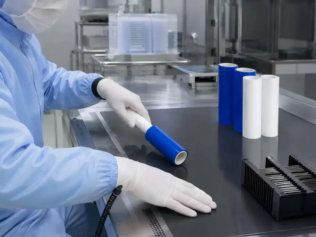
At Nabai, we configure each Sticky Roller for Semiconductor project around the intended contact surface and contamination risk. The objective is controlled removal of loose, dry particles—not maximum adhesion in every situation.
What Adhesion Data Actually Means
Adhesion is commonly reported as peel force per unit width, such as g/25 mm. However, a value is meaningful only when the test substrate, peel angle, conditioning, dwell time, and test speed are defined. ASTM D3330/D3330M covers peel-adhesion measurement for pressure-sensitive tapes and supports comparisons of adhesion uniformity. Therefore, two rollers carrying the same numerical value may perform differently when tested under different conditions. nt, specify:
•Test method and peel angle
•Reference substrate
•Conditioning temperature and humidity
•Test speed and dwell time
•Acceptable average and tolerance
•Residue and particle-shedding requirements
ISO 14644-1 classifies cleanrooms by airborne particle concentration; it does not prescribe an adhesion grade for a Sticky Roller for Semiconductor use. Adhesion must therefore be selected through application-specific testing. sion Ranges and Typical Uses
The following ranges represent configurable Nabai product options rather than universal semiconductor standards.
| Nabai Adhesion Range | Recommended Starting Point | Typical Approved Surfaces |
| 250–350 g/25 mm | Low tack | Protective films, smooth polymer trays, coated panels, and easily marked surfaces |
| 350–450 g/25 mm | Medium tack | Workbenches, equipment covers, carrier exteriors, tool carts, and general cleanroom surfaces |
| 450–550 g/25 mm | High tack | Durable metal fixtures, rigid housings, and surfaces carrying heavier fibers or visible loose debris |
A Sticky Roller for Semiconductor processes should not automatically be applied to active wafer surfaces, reticle or photomask faces, sensor windows, or functional optical coatings. Direct contact with these critical surfaces requires written process approval and compatibility validation.
Five Factors That Determine the Correct Adhesion Level
1. Surface Contact Adhesive Sensitivity
Low tack options are best for bonding soft polymers, coated glass and painted surfaces. When bonding labels and thin films to anodized surfaces and stainless steel, use mediums to high tack adhesives. Consider any potential cosmetic effects and residue.
2. Particle Type and Loading
The Sticky Roller for Semiconductors is highly effective for the collection of loose dust, lint, fibers, and other dry particulates. Although higher tack may enhance collection of larger particulates, capture of smaller particulates or particulate adhered to chemical films or dried residue from process chemicals should not be accomplished through the replacement of a validated cleaning procedure.
3. Residue and Material Compatibility
Evaluate the roller on the actual production surface. Inspection should cover:
•Visible adhesive transfer
•Haze or gloss change
•Surface marking or coating lift
•Particle redeposition
•Performance after repeated passes
4. Electrostatic Risk
Adhesion and electrostatic performance are separate specifications. IEC 61340-5-1:2024 requires an organized ESD control program; it does not classify a roller as ESD-safe based only on a stated resistance value. A Sticky Roller for Semiconductor used inside an electrostatic protected area should be assessed as part of the complete system, including the operator, handle, roller, work surface, grounding path, and verification procedure. configurations, a typical declared surface-resistivity range may be 10⁶–10⁹ Ω/sq, subject to the agreed test method. The inspection report should identify:
•Component being measured
•Instrument and electrode arrangement
•Test temperature and humidity
•Measurement method
•Reporting unit and acceptance range
5. Cleaning Frequency and Layer Life
Do not compensate for an overloaded sheet by selecting excessive tack. Replace or peel the contaminated layer when pickup efficiency declines or embedded debris could scratch the next surface. A fresh medium-tack sheet is often safer than repeatedly using a saturated high-tack sheet.
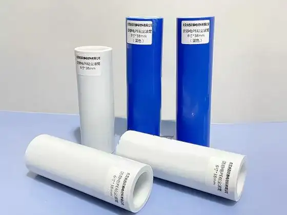
Nabai ESD-Safe PE Sticky Roller Configuration
A Nabai Sticky Roller for Semiconductor can be customized according to the process requirement.
| Parameter | Available Configuration |
| Adhesive range | 250–550 g/25 mm under agreed test conditions |
| Roller film | Low-lint PE adhesive sheet |
| Handle and core | PP or PE configuration, depending on design |
| ESD option | Carbon-modified or static-dissipative construction |
| Width | 4, 6, 8, 10, or 12 inches; custom sizes available |
| Core diameter | 25.4, 38, 50.8, or 76 mm |
| Colors | White, blue, transparent, or grey |
A smooth-bearing handle helps maintain even pressure and consistent surface contact. Nevertheless, mechanical design does not replace operator training or process validation.
Proposed Qualification Procedure
Nabai suggests a trial under controlled conditions before allowing a Sticky Roller to be used in Semiconductor manufacturing.
•Low-, medium-, and high-tack samples should be taken.
•These should be tested on real surfaces that are non-critical and representative.
•A specified amount of passes at set pressures should be used.
•The removal of particles should be assessed using the approved inspection method of the facility.
•Assess for residue, alteration of surface, shedding and change in charge behavior.
•Record the selected grade and operating limits in the cleaning SOP.
Choosing Adhesion Without Adding New Risk
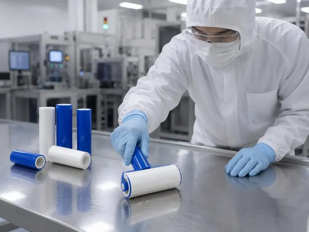
The correct Sticky Roller for Semiconductor solution is the lowest adhesion level that reliably removes target particles without leaving residue, damaging the surface, or disrupting ESD controls.
Nabai's customizable range of 250–550 g/25 mm provides a practical starting point, but final selection should be based on a documented test method and production-surface qualification. By treating tack, cleanliness, material compatibility, and electrostatic control as separate but connected requirements, semiconductor facilities can establish a more repeatable and defensible roller-cleaning process.
FAQs
Q1. What level of adhesion should a Sticky Roller for Semiconductor use have?
A level of Medium adhesion is applicable for several cleaning requirements, however, the final level should be tested on the actual surface.
Q2. Is a higher adhesion level always more effective?
Not always. Higher levels of adhesion may result in increased residue, surface marking, and damage risks to the coating.
Q3. What is low adhesion Sticky Roller suitable for?
It is mainly considered for use on protective films, coated panels, polymer trays, and other sensitive surfaces.
Q4. Can a Sticky Roller for Semiconductor clean wafers directly?
We do not recommend direct wafer contact without the specific validation of the roller and cleaning process.
Q5. Can Nabai customize the adhesion strength?
Yes. Nabai can configure adhesion within the specified product range according to surface and process requirements.
NEWS
GET SERVICE
With quality parts to meet every budget and friendly staff trained to make your visit informative and hassle free.